Laser patterning of functional materials represents an innovative technology with the capability to deliver meticulous and efficient patterning on a wide range of materials. This advanced method has found practical applications across various industries, including electronics, optics, microfluidics, and biomedical engineering. Through harnessing the potential of laser beams, researchers and engineers can craft highly personalized, high-resolution patterns with exceptional precision.
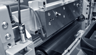
The slot-die coating process employs a slot-die head, composed of a narrow slit orifice, typically constructed from top-quality materials like stainless steel. This specialized head is engineered to maintain a precise gap between its front and back, ensuring consistency. The coating material is then pumped into the slot-die head, flowing through the narrow slit to create a uniform film as it covers the substrate.
Laser patterning is an advanced technique that harnesses laser radiation to intricately modify materials, creating precise patterns. The interaction between the laser and the material is influenced by key parameters such as wavelength, power, and focus.
Materials exhibit diverse responses to laser patterning: ablation removes layers, melting leads to fusion, and chemical changes can take place. This adaptability makes laser patterning suitable for a wide array of functional materials, spanning from semiconductors to biomaterials.
In the realms of manufacturing, research, and development, laser patterning plays a pivotal role, empowering precise material structuring with unmatched control.
Laser technology offers a host of advantages, with one standout feature being its non-contact approach. This eliminates the requirement for physical masks or direct material contact, thereby reducing the risks associated with contamination, damage, or wear during the patterning process.
Lasers excel in delivering exceptional precision and resolution, making it possible to create intricate patterns with feature sizes as small as micrometers or even nanometers. This level of precision proves indispensable for applications that demand miniaturization, such as integrated circuits and microfluidic devices.
Laser patterning, when combined with manufacturing methods like thin film deposition or etching, creates multifunctional devices and structures. Integrating laser patterning with additive or subtractive techniques leads to complex, personalized functional materials in areas like optoelectronics, sensors, and microfluidics.
It's a powerful technique for precise, efficient pattern fabrication, propelling us into the future of advanced materials and technology.